
As environmental regulations become stricter and sustainability gains importance across industries, electronics manufacturers are increasingly adopting environmentally responsible production practices. One of the most significant developments in this area is lead free PCB assembly, a manufacturing process that eliminates the use of lead-based solder in printed circuit board assembly. This approach not only helps companies comply with global environmental regulations but also supports safer products and more sustainable manufacturing operations.
Today, lead free PCB assembly has become the industry standard for many consumer electronics, automotive systems, medical devices, telecommunications equipment, and industrial products. Understanding the process, advantages, challenges, and applications of lead-free assembly is essential for businesses involved in electronics design and manufacturing.
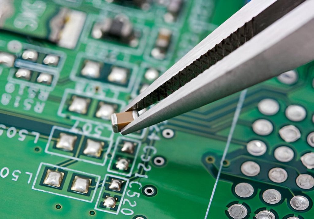
What Is Lead Free PCB Assembly?
Lead free PCB assembly is the process of assembling electronic components onto printed circuit boards using solder alloys that do not contain lead (Pb). Traditional solder materials typically consisted of a tin-lead alloy, commonly known as SnPb solder. While effective and reliable, lead-based solder poses environmental and health risks because lead is a toxic heavy metal.
To address these concerns, manufacturers began adopting lead-free solder alloys, which are typically composed of tin combined with silver, copper, bismuth, or other metals. The most widely used lead-free solder alloy is SAC (Tin-Silver-Copper), which provides excellent mechanical and electrical performance.
Lead free PCB assembly is now widely used to meet environmental standards such as the Restriction of Hazardous Substances (RoHS) directive and other international regulations.
Why Lead Free PCB Assembly Is Important
The importance of lead-free PCB assembly extends beyond regulatory compliance. Environmental protection is one of the primary reasons for its widespread adoption.
Lead can accumulate in soil, water, and living organisms, creating long-term environmental and health concerns. By eliminating lead from electronic products, manufacturers help reduce the environmental impact of electronic waste.
Consumer safety is another important factor. Lead-free products reduce the risk of exposure during manufacturing, usage, recycling, and disposal.
In addition, many global markets require RoHS-compliant products. Companies that fail to adopt lead-free manufacturing processes may face restrictions when selling products internationally.
As sustainability becomes a competitive advantage, lead free PCB assembly helps organizations demonstrate their commitment to responsible manufacturing practices.
Materials Used in Lead Free PCB Assembly
The success of lead free PCB assembly depends heavily on selecting the right materials.
Lead-free solder alloys are the most important materials used in the process. SAC305, which consists of approximately 96.5% tin, 3% silver, and 0.5% copper, is one of the most common choices due to its reliability and performance.
Other lead-free solder formulations may include bismuth, antimony, or nickel to achieve specific performance characteristics.
Lead-free solder pastes are used during surface mount assembly to secure components to the PCB.
PCB surface finishes such as ENIG (Electroless Nickel Immersion Gold), immersion silver, immersion tin, and OSP (Organic Solderability Preservative) are often selected for compatibility with lead-free soldering processes.
The materials used must work together to ensure strong solder joints, long-term reliability, and compliance with industry standards.
Lead Free PCB Assembly Process
The lead free PCB assembly process follows many of the same steps as conventional PCB assembly but requires careful control of temperatures and materials.
The process begins with solder paste printing, where lead-free solder paste is applied to designated component pads using a precision stencil.
Surface mount technology (SMT) equipment then places electronic components onto the PCB with high accuracy.
The board passes through a reflow oven, where carefully controlled heating profiles melt the solder paste and create permanent electrical connections. Lead-free solder requires higher reflow temperatures compared to traditional lead-based solder.
For through-hole components, wave soldering or selective soldering may be used with lead-free solder alloys.
After assembly, the boards undergo inspection and testing procedures, including Automated Optical Inspection (AOI), X-ray inspection, in-circuit testing, and functional testing.
These quality assurance measures ensure that the assembled boards meet performance and reliability requirements.
Benefits of Lead Free PCB Assembly
One of the primary advantages of lead free PCB assembly is environmental compliance. Manufacturers can meet RoHS, WEEE, and other regulatory requirements that restrict hazardous substances in electronic products.
Improved sustainability is another significant benefit. Lead-free manufacturing helps reduce environmental pollution and supports responsible recycling practices.
Many lead-free solder alloys also offer excellent mechanical strength, improving resistance to vibration and thermal cycling in certain applications.
Consumer confidence can be enhanced as customers increasingly prefer environmentally friendly products.
Lead-free assembly also enables manufacturers to access global markets where environmental compliance is mandatory.
These advantages have made lead free PCB assembly the preferred choice for many electronics manufacturers worldwide.
Challenges of Lead Free PCB Assembly
Despite its benefits, lead free PCB assembly presents several technical challenges.
One of the most notable challenges is the higher melting temperature of lead-free solder. This requires increased reflow temperatures, which can place additional stress on components and PCB materials.
Process control becomes more critical because temperature profiles must be carefully optimized to prevent solder defects.
Some lead-free solder alloys may exhibit different wetting characteristics compared to traditional lead-based solders, requiring adjustments in manufacturing processes.
Material compatibility is also important. PCB laminates, surface finishes, and components must be capable of withstanding the higher processing temperatures associated with lead-free assembly.
Manufacturers must invest in proper equipment, training, and quality control systems to successfully implement lead-free production.
Applications of Lead Free PCB Assembly
The use of lead free PCB assembly has expanded across virtually every sector of the electronics industry.
Consumer electronics manufacturers rely on lead-free assembly for smartphones, tablets, laptops, televisions, gaming devices, and smart home products.
Automotive electronics increasingly utilize lead-free PCB assembly in control units, sensors, infotainment systems, and electric vehicle technologies.
Medical devices benefit from lead-free assembly due to strict regulatory requirements and safety considerations.
Industrial automation equipment, telecommunications infrastructure, and networking hardware also commonly use lead-free assembly processes.
Aerospace and defense applications are gradually adopting lead-free technologies where appropriate, although certain specialized applications may still require exemptions.
The broad adoption of lead-free assembly demonstrates its effectiveness across diverse industries.
Quality Control in Lead Free PCB Assembly
Maintaining quality is essential in lead free PCB assembly because solder joint integrity directly affects product reliability.
Automated Optical Inspection systems are used to identify soldering defects, component placement errors, and assembly inconsistencies.
X-ray inspection helps evaluate hidden solder joints in complex packages such as BGAs and QFNs.
Solder joint analysis is often performed to verify proper wetting and structural integrity.
In-circuit testing and functional testing ensure that the assembled board performs according to design specifications.
Thermal cycling and reliability testing may also be conducted for products intended for demanding operating environments.
These quality assurance measures help manufacturers achieve consistent and dependable results.
Future Trends in Lead Free PCB Assembly
The future of lead free PCB assembly is closely connected to advancements in sustainable manufacturing and electronics innovation.
New solder alloy formulations are being developed to improve reliability, reduce processing temperatures, and enhance environmental performance.
Automation and artificial intelligence are helping manufacturers optimize production processes and improve defect detection.
As electronic devices become smaller and more complex, lead-free assembly technologies will continue to evolve to support advanced packaging and miniaturization requirements.
The growing emphasis on environmental responsibility will further accelerate the adoption of lead-free manufacturing worldwide.
Conclusion
Lead free PCB assembly has transformed modern electronics manufacturing by providing a safer, more environmentally responsible alternative to traditional lead-based soldering processes. By supporting regulatory compliance, reducing environmental impact, and delivering reliable performance, lead-free assembly has become a critical component of sustainable electronics production.
As global regulations continue to evolve and demand for eco-friendly products increases, lead-free manufacturing will remain an essential industry standard. Companies seeking high-quality, compliant, and reliable production solutions often partner with a trusted lead-free PCB assembly service provider to ensure consistent quality, environmental responsibility, and long-term product success.